I’d like to output the clock signal directly from a Shrike pin in order to provide it to another board.
I tried the code below.
“assign clk_pin = clk;”
It passed compilation and bitstream generation.
However, it did not output any signal.
Could you tell me how to solve this issue?
Any advice would be appreciated.
Hii @tomoya_yanagida ,
The Verilog statement assign clk_pin = clk; is syntactically valid and, by itself, should allow the input clock to be driven to an output pin. However, on the SLG47910, please also verify that the output-enable signal for the pin is asserted (for example, assign clk_pin_en = 1'b1; if your design uses a separate OE signal) and that both the output signal and its OE are correctly assigned in the I/O Planner.
I want to know how much frequency you are generating by clk (if you use it from osc directly it will be 50Mhz or else if you generate ant other freq using PLL, then what is your freq?).
Since, if the hardware configuration is correct but you are verifying the signal with a logic analyzer, please let me know the analyzer model and sampling rate. A 50 MHz clock cannot be reliably measured with a 16–24 MS/s logic analyzer, which may display an incorrect frequency, a constant level, or no apparent clock due to aliasing. If possible, try outputting a divided clock or verify the signal with an oscilloscope.
Thank you for your reply.
Sorry for the late reply.
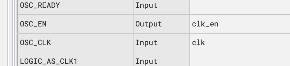
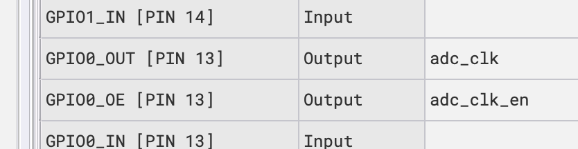
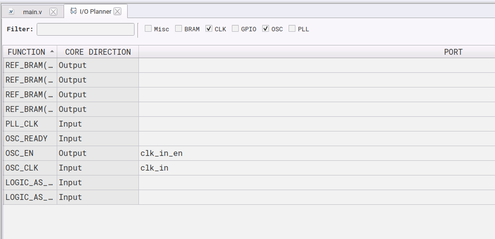
The image below shows my pin assignments.
My Verilog code is as follows:
(* top ) module top (
// FPGA internal clock
( iopad_external_pin, clkbuf_inhibit ) input wire clk,
( iopad_external_pin ) output wire clk_en,
( iopad_external_pin ) output wire adc_clk,
( iopad_external_pin *) output wire adc_clk_en // connect to external ADC clock pin
);
assign clk_en  = 1'b1;
assign adc_clk_en = 1'b1;
assign adc_clk = clk;
endmodule
What do you think? Does anything look incorrect, or is there something I might be missing?
Thank you very much for your help.
Your logic is fine, It will generate the 50MHz clock from the GPIO0 pin number (F0). Make sure that, you are taking output from this pin.
Can I know how did you check that the output clock is generating or not? I mean did you use any logic analyser? if yes which logic analyser??
I used an oscilloscope to check the output signal.
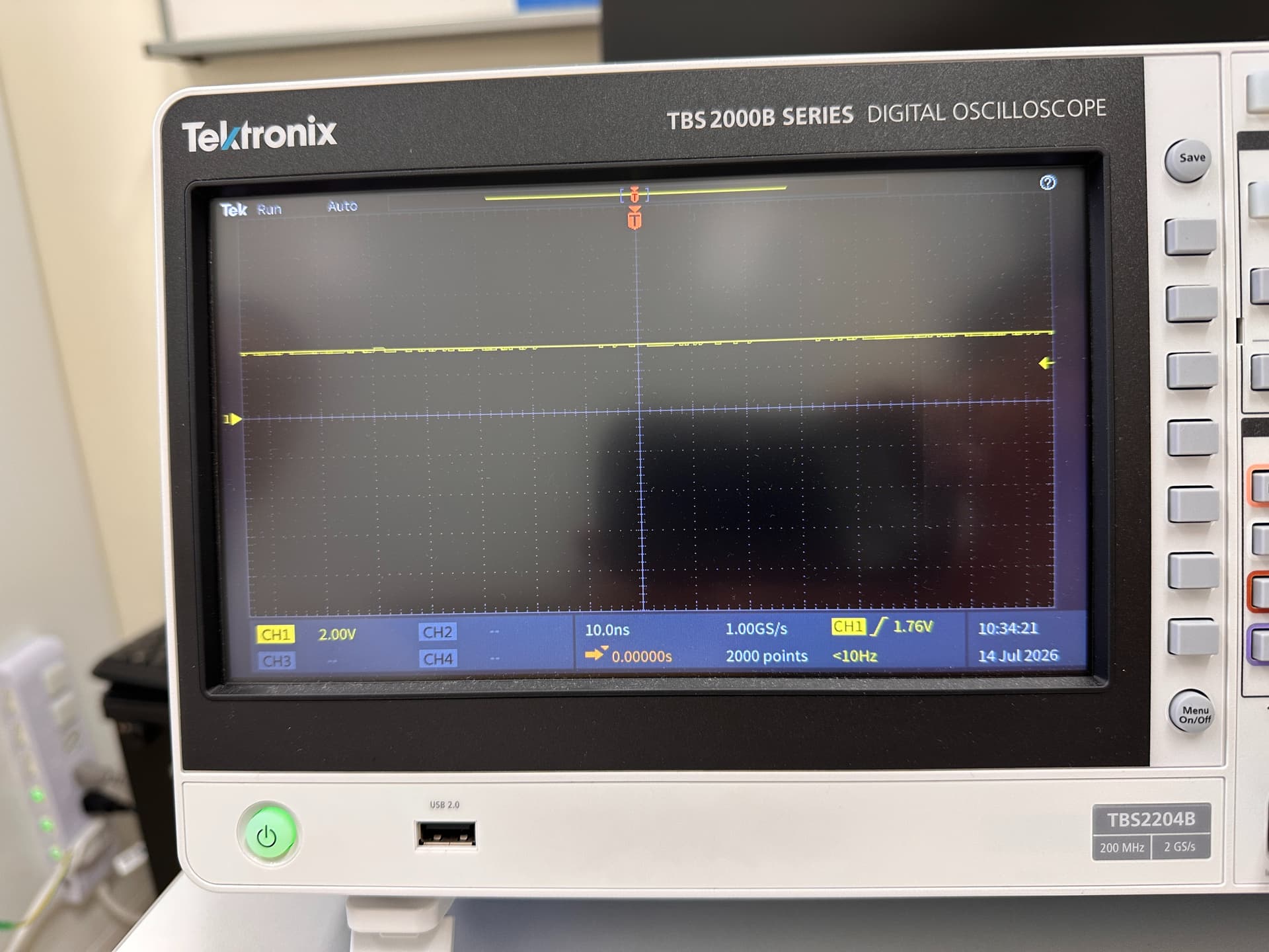
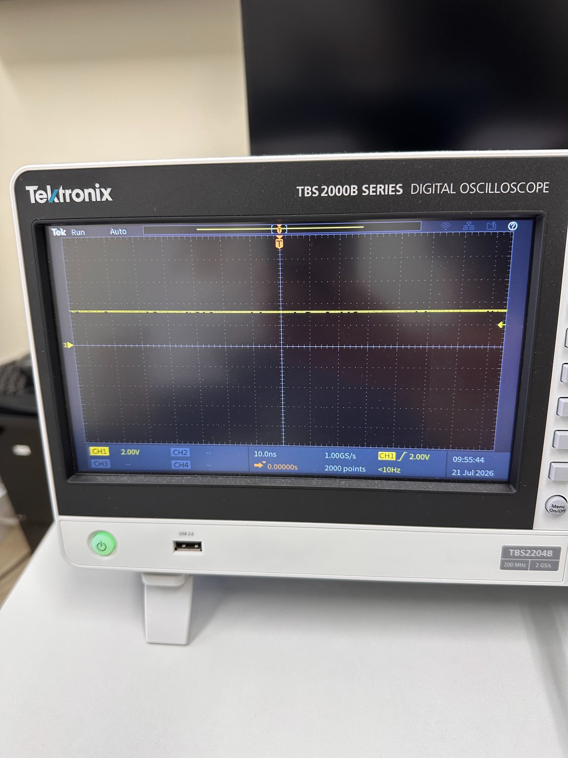
With the original code, I observed the following waveform on the GPIO0 (F0) pin:
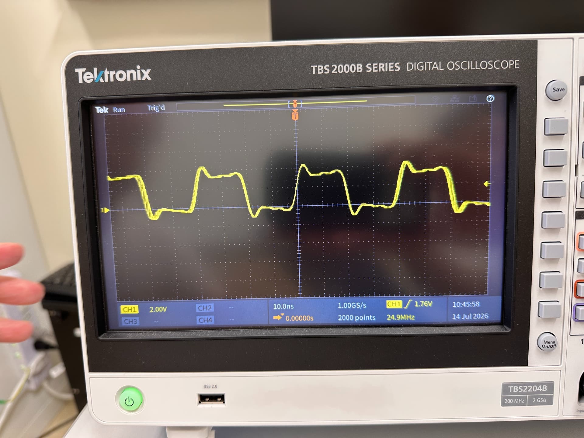
However, when I modified the Verilog code so that adc_clk toggles on every rising edge of the internal clock, the signal was observed correctly on the oscilloscope:
(* top *) module top (
    // FPGA internal clock
    (* iopad_external_pin, clkbuf_inhibit *) input  wire clk,
    (* iopad_external_pin *) output wire clk_en,
    (* iopad_external_pin *) output reg  adc_clk,
    (* iopad_external_pin *) output wire adc_clk_en
);

    wire rst_n;

    assign clk_en     = 1'b1;
    assign adc_clk_en = 1'b1;
    assign rst_n      = 1'b1;

    always @(posedge clk or negedge rst_n) begin
        if (!rst_n)
            adc_clk <= 1'b0;
        else
            adc_clk <= ~adc_clk;
    end

endmodule
I output this signal from the same GPIO0 (F0) pin and observed the following waveform:
This suggests that the GPIO pin itself is working correctly. However, I am still unable to obtain the expected 50 MHz clock waveform when directly assigning clk to adc_clk.
Do you have any idea what might be causing this issue?
I got the issue, The issue is that when you directly assign clk to adc_clk (for first case, assign adc_clk = clk;), the synthesis tool may optimize away the input clock because it is not used by any internal logic in the design. As a result, the clock is not routed, and no signal appears on the output pin.
That’swhy, in your second case when you use your input clock, it’s able to generate the input clock and outputs the 25Mhz, based on your internal logic.
To prevent this optimization, use the input clock in some internal logic, even if it is just a simple operation (for example, a counter or a flip-flop). Once the clock is actually used in the design, the synthesis tool will preserve and route it, and it can then be assigned to the output pin.
This should resolve the issue.
Thank you for your explanation.
I tried using the input clock in internal logic by adding a flip-flop, as you suggested. However, I encountered a compilation error when I built the design.
I used the following code:
(* top ) module top (
// FPGA internal clock
( iopad_external_pin, clkbuf_inhibit ) input wire clk,
( iopad_external_pin ) output wire clk_en,
( iopad_external_pin ) output reg adc_clk,
( iopad_external_pin *) output wire adc_clk_en // connect to external ADC clock pin
);
wire rst_n;
reg dummy;

assign clk_en  = 1'b1;
assign adc_clk_en = 1'b1;
assign rst_n = 1'b1;
always @(posedge clk or negedge rst_n) begin
dummy <= ~dummy;
end
assign adc_clk = clk;
endmodule
The compiler returned the following error:
[ERROR (Synthesis): Multiple edge sensitive events found for this signal! ]
Is there anything wrong with this implementation, or is there a specific constraint or method required to use the input clock with this FPGA?
Thank you for your help.
Hello @tomoya_yanagida ,
In your logic some of the issues are there. It’s seems like you are not familiar with verilog.
In your logic you have two edge-sensitive events (posedge clk and negedge rst_n), which is normally used for an asynchronous reset. However, your code never actually uses rst_n inside the block. Also rst_n is permanently tied high, so it will never have a negative edge. This is the reason for the error.
One more thing is you declared the output reg adc_clk and had assigned that with continuous block, which is illegal (reg data type only use in procedural block).
You can use this logic that it will generate the 50Mhz output clock:
(* top *) module top (
    (* iopad_external_pin *) input wire clk,
    (* iopad_external_pin *) output wire clk_en,
    (* iopad_external_pin *) output wire adc_clk,
    (* iopad_external_pin *) output wire adc_clk_en
);

reg dummy;

assign clk_en     = 1'b1;
assign adc_clk_en = 1'b1;
assign adc_clk    = clk;

always @(posedge clk) begin
    dummy <= ~dummy;
end

endmodule
Please make sure that to give the pin names and pin numbers in the IO planner correctly. This should works.
Thank you for your help.
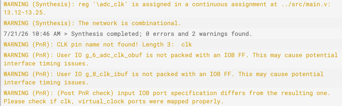
I checked the pin assignments and tried running the code you provided. However, I encountered the issue shown in the image below.
Also, could the warning shown in the second image be related to this issue?
Hello @tomoya_yanagida,
I think you are not using the logic that I have mentioned in the previous reply. Please use that logic and retry. That should work.
In this case, your design becomes combinational design as it’s not using any clock.
One more thing, please give same pin names in the IO planner that you are mentioning in the code.
Please recheck and let me know the status, If you still faces any issue, I will create that project and will share that.
nice Tektronix scope btw.
Hello,
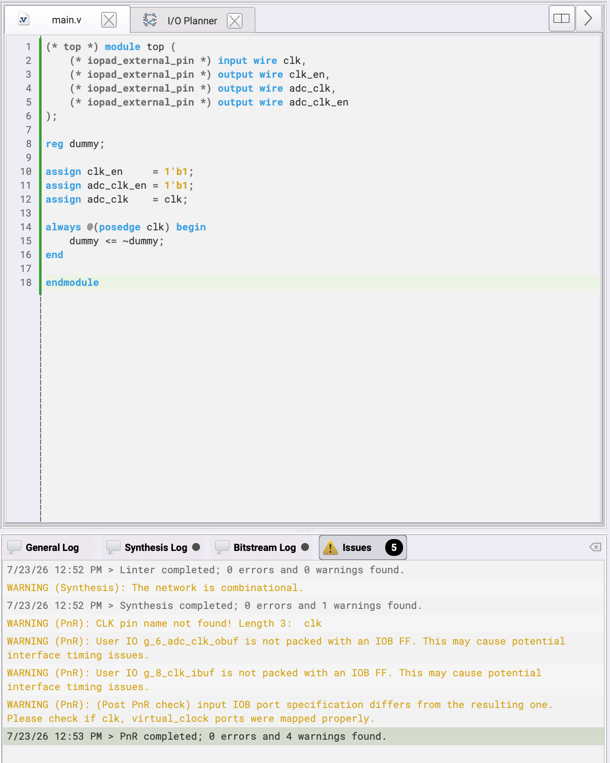
I used the code you provided and confirmed that the pin assignments in the IO Planner match the pin names used in the code. I then checked the output again using an oscilloscope, but I obtained the same result as before.
Here are the code and the warning messages.
It should work, I think you are missing something in your design, May be you are not assigning the pin numbers correctly.
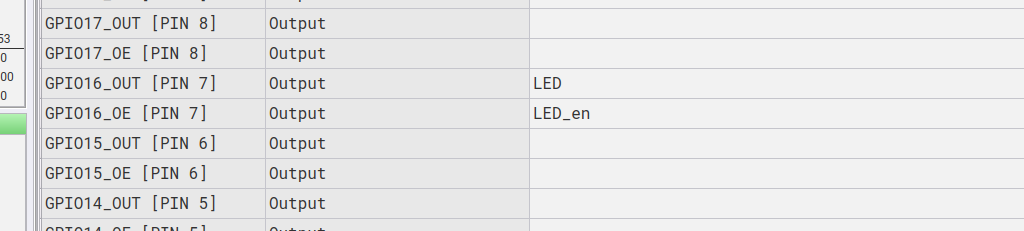
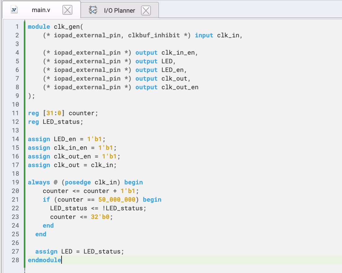
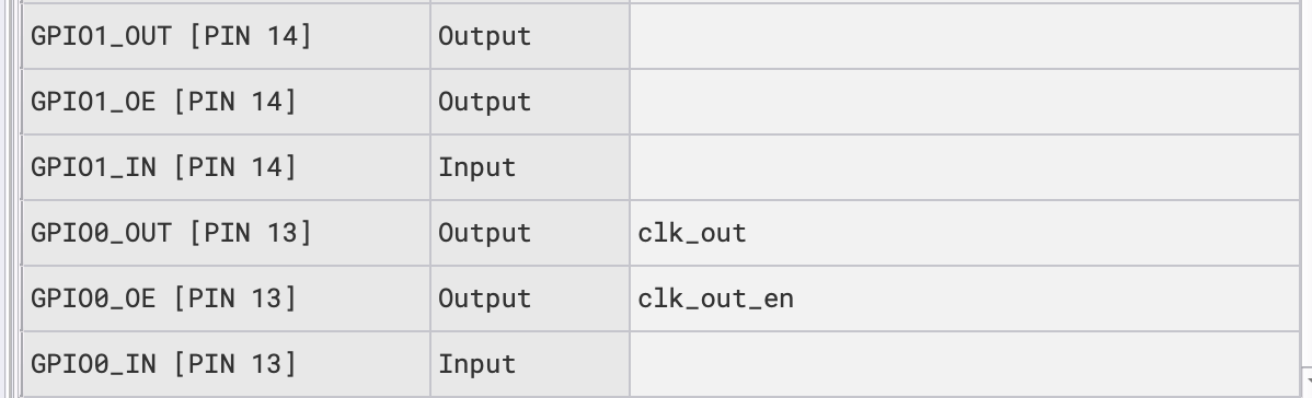
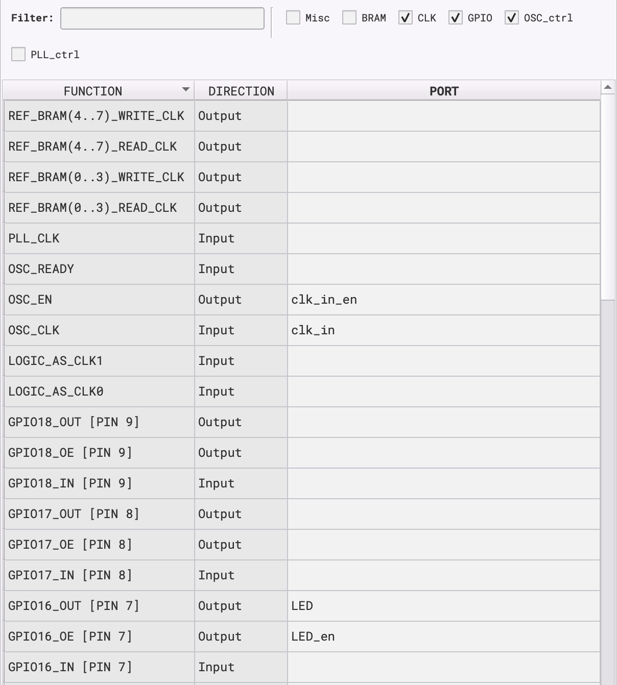
Let’s do one thing, We can add the LED blink logic in our logic, so that, it will generates our required clock and also confirms that whether you are following correct steps or not.
This is the code you have to use and the pin mappings you have to do.
(*top*) module clk_gen(
	(* iopad_external_pin, clkbuf_inhibit *) input clk_in,

    (* iopad_external_pin *) output clk_in_en,
	(* iopad_external_pin *) output LED,
  	(* iopad_external_pin *) output LED_en,
    (* iopad_external_pin *) output clk_out,
    (* iopad_external_pin *) output clk_out_en
);

reg [31:0] counter;
reg LED_status;

assign LED_en = 1'b1;
assign clk_in_en = 1'b1;
assign clk_out_en = 1'b1;
assign clk_out = clk_in;

always @ (posedge clk_in) begin
    counter <= counter + 1'b1;
    if (counter == 50_000_000) begin
      LED_status <= !LED_status;
      counter <= 32'b0;
    end
  end

  assign LED = LED_status;
endmodule
Make sure that you are assigning the pin numbers with same pin names as mentioned above.
1 Like
I made sure that the signal names in the program code matched those in the pin assignments, as you suggested. However, I still obtained the same result as before, and the LED did not blink either.
Everything seems correct in the above design, LED should blink and clk_out should also generate, if you flash the bitstream successfully. Can I know the how did you program the FPGA? And are you sure you are flashing the updated bitstream only?? If you try to flash the old bitstream then you might get face the issue.